- 您现在的位置:买卖IC网 > Sheet目录330 > IDT71V432S5PFGI (IDT, Integrated Device Technology Inc)IC SRAM 1MBIT 5NS 100TQFP
�� �
�
�IDT71V432,� 32K� x� 32� CacheRAM�
�3.3V� Synchronous� SRAM� with� Burst� Counter,� Single� Cycle� Deselect�
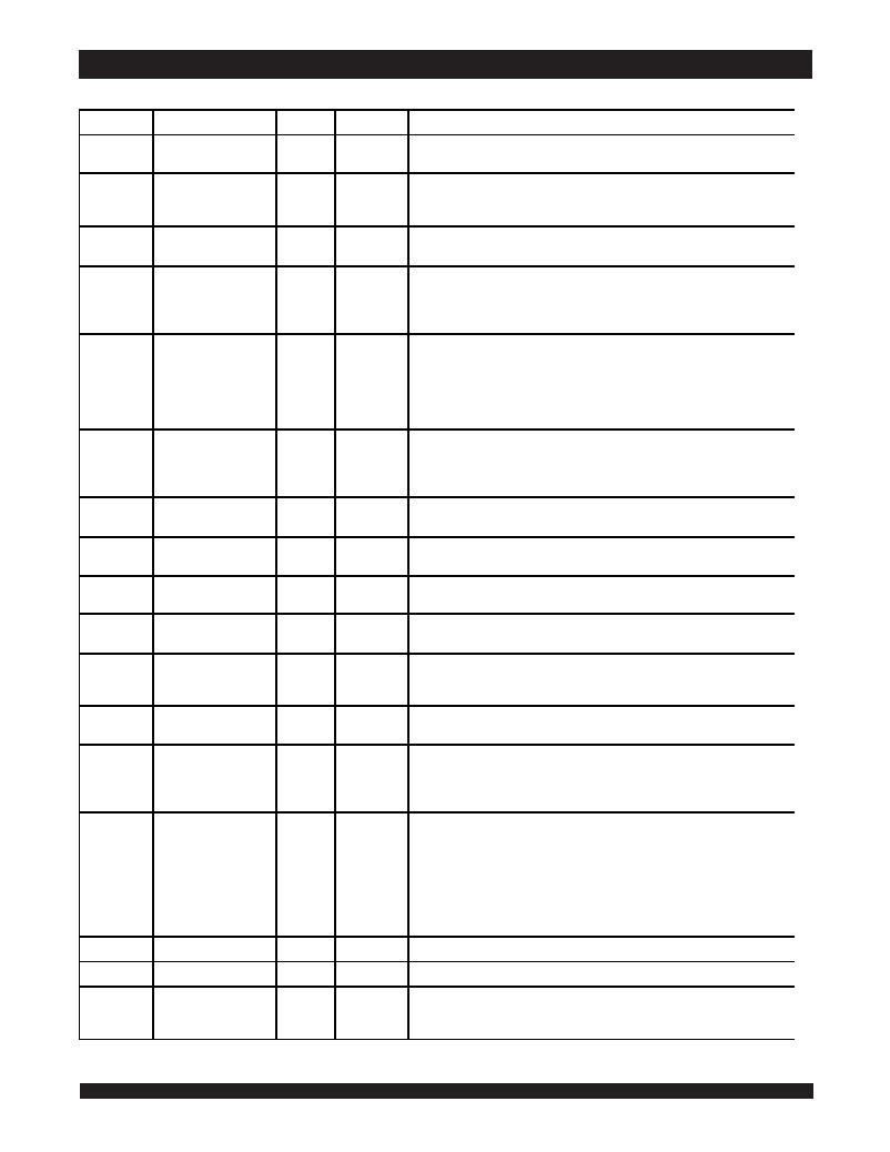
�Pin� Definitions� (1)�
�Commercial� and� Industrial� Temperature� Ranges�
�Symbol�
�A� 0� –A� 14�
�Pin� Function�
�Address� Inputs�
�I/O�
�I�
�Active�
�N/A�
�Description�
�Synchronous� Address� inputs.� The� address� re� gister� is� triggered� by� a� combination�
�of� the� rising� edge� of� CLK� and� ADSC� Low� or� ADSP� Low� and� CE� Low.�
�ADSC�
�Address� Status�
�I�
�LOW�
�Sy� nchronous� Ad� dress� Status� from� Cache� Controller.� ADSC� is� an� active� LOW�
�(Cache� Controller)�
�input� that� is� used� to� load� the� address� registers� with� new� addresses.� ADSC� is�
�NOT� GATED� by� CE� .�
�ADSP�
�ADV�
�Address� Status�
�(Processor)�
�Burst� Address� Advance�
�I�
�I�
�LOW�
�LOW�
�Synchronous� Address� Status� from� Processor.� ADSP� is� an� active� LOW� input� that� is�
�used� to� load� the� address� registers� with� new� addresses.� ADSP� is� gated� by� CE� .�
�Synchronous� Address� Advance.� ADV� is� an� active� LOW� input� that� is� used� to�
�advance� the� internal� burst� counter,� co� ntrolling� burst� access� after� the� initial�
�address� is� loaded.� When� this� input� is� HIGH� the� burst� counter� is� not� incremented;�
�that� is,� there� is� no� address� advance.�
�BWE�
�Byte� Write� Enable�
�I�
�LOW�
�Synchronous� byte� write� enable� gates� the� byte� write� inputs� BW� 1� –� BW� 4� .� If� BWE� is�
�LOW� at� the� rising� edge� of� CLK� then� BW� X� inputs� are� passed� to� the� next� stage� in�
�the� circuit.� A� byte� write� can� still� be� blocked� if� ADSP� is� LOW� at� the� rising� edge� of�
�CLK.� If� ADSP� is� HIGH� and� BW� X� is� LOW� at� the� rising� edge� of� CLK� then� data� will�
�be� written� to� the� SRAM.� If� BWE� is� HIGH� then� the� byte� write� inputs� are� blocked�
�and� only� GW� can� initiate� a� write� cycle.�
�BW� 1� -� BW� 4�
�Individual� Byte�
�Write� Enables�
�I�
�LOW�
�Synchronous� byte� write� enables.� BW� 1� controls� I/O(7:0),� BW� 2� controls� I/O(15:8),�
�etc.� Any� active� byte� write� causes� all� outputs� to� be� disabled.� ADSP� LOW�
�disables� all� byte� writes.� BW� 1� –� BW� 4� must� meet� specified� setup� and� hold� times�
�with� respect� to� CLK.�
�CE�
�Chip� Enable�
�I�
�LOW�
�Synchronous� chip� enable.� CE� is� used� with� CS� 0� and� CS� 1� to� enable� the�
�IDT71V432.� CE� also� gates� ADSP� .�
�CLK�
�Clock�
�I�
�N/A�
�This� is� the� clock� input� to� the� IDT71V432.� All� timing� referenc� es� for� the� device� are�
�made� with� respect� to� this� input.�
�CS� 0�
�Chip� Select� 0�
�I�
�HIGH�
�Synchronous� active� HIGH� chip� select.� CS� 0� is� used� with� CE� and� CS� 1� to� enable�
�the� chip.�
�CS� 1�
�Chip� Select� 1�
�I�
�LOW�
�Sy� nchronous� active� LOW� chip� select.� CS� 1� is� used� with� CE� and� CS� 0� to� enable�
�the� chip.�
�GW�
�Global� Write� Enable�
�I�
�LOW�
�Synchronous� global� write� enable.� This� input� will� write� all� four� 8-bit� data� bytes�
�when� LOW� on� the� rising� edge� of� CLK.� GW� supercedes� individual� byte� write�
�enables.�
�I/O� 0� –I/O� 31�
�Data� Input/Output�
�I/O�
�N/A�
�Synchronous� data� input/output� (I/O)� pins.� Both� the� data� input� path� and� data� output�
�path� are� registered� and� triggered� by� the� rising� edge� of� CLK.�
�LBO�
�Linear� Burst� Order�
�I�
�LOW�
�Asynchronous� burst� order� sele� ction� DC� input.� When� LBO� is� HIGH� the� Interleaved�
�(Intel)� burst� sequence� is� selected.� When� LBO� is� LOW� the� Linear� (PowerPC)� burst�
�sequence� is� selected.� LBO� is� a� static� DC� input� and� must� not� change� state� while�
�the� device� is� operating.�
�OE�
�Output� Enable�
�I�
�LOW�
�Asynchronous� output� enable.� When� OE� is� LOW� the� data� output� drivers� are�
�enabled� on� the� I/O� pins.� OE� is� gated� internally� by� a� delay� circuit� driven� by� CE� ,�
�CS� 0� ,� and� CS� 1� .� In� dual-bank� mode,� when� the� user� is� utilizing� two� banks� of�
�IDT71V432� and� toggling� back� and� forth� between� them� using� CE� ,� the� internal�
�de� lay� circuit� delays� the� OE� activation� of� the� data� output� drivers� by� one� cycle� to�
�prevent� bus� contention� between� the� banks.� When� used� in� single� bank� mode� CE� ,�
�CS� 0� ,� and� CS� 1� are� all� tied� active� and� there� is� no� output� enable� delay.� When� OE� is�
�HIGH� the� I/O� pins� are� in� a� high-impedence� state.�
�V� DD�
�V� SS�
�ZZ�
�Power� Supply�
�Ground�
�Sleep� Mode�
�N/A�
�N/A�
�I�
�N/A�
�N/A�
�HIGH�
�3.3V� power� supply� inputs.�
�Ground� pins.�
�Asynchronous� sleep� mode� input.� ZZ� HIGH� will� gate� the� CLK� internally� and� power�
�down� the� IDT71V432� to� its� lowest� power� consumption� level.� Data� retention� is�
�guaranteed� in� Sleep� Mode.�
�NOTE:�
�1.� All� synchronous� inputs� must� meet� specified� setup� and� hold� times� with� respect� to� CLK.�
�6.42�
�3104� tbl� 02�
�发布紧急采购,3分钟左右您将得到回复。
相关PDF资料
IDT71V546S133PFGI
IC SRAM 4MBIT 133MHZ 100TQFP
IDT71V547S80PFGI
IC SRAM 4MBIT 80NS 100TQFP
IDT71V632S7PFGI
IC SRAM 2MBIT 7NS 100TQFP
IDT71V65703S85BGGI
IC SRAM 9MBIT 85NS 119BGA
IDT71V65803S150BGI
IC SRAM 9MBIT 150MHZ 119BGA
IDT71V67602S166BGG
IC SRAM 9MBIT 166MHZ 119BGA
IDT71V67603S166PFGI
IC SRAM 9MBIT 166MHZ 100TQFP
IDT71V67703S85BGGI
IC SRAM 9MBIT 85NS 119BGA
相关代理商/技术参数
IDT71V432S5PFGI8
功能描述:IC SRAM 1MBIT 5NS 100TQFP RoHS:是 类别:集成电路 (IC) >> 存储器 系列:- 标准包装:72 系列:- 格式 - 存储器:RAM 存储器类型:SRAM - 同步 存储容量:4.5M(256K x 18) 速度:133MHz 接口:并联 电源电压:3.135 V ~ 3.465 V 工作温度:0°C ~ 70°C 封装/外壳:100-LQFP 供应商设备封装:100-TQFP(14x20) 包装:托盘
IDT71V432S6PF
功能描述:IC SRAM 1MBIT 6NS 100TQFP RoHS:否 类别:集成电路 (IC) >> 存储器 系列:- 标准包装:576 系列:- 格式 - 存储器:闪存 存储器类型:闪存 - NAND 存储容量:512M(64M x 8) 速度:- 接口:并联 电源电压:2.7 V ~ 3.6 V 工作温度:-40°C ~ 85°C 封装/外壳:48-TFSOP(0.724",18.40mm 宽) 供应商设备封装:48-TSOP 包装:托盘 其它名称:497-5040
IDT71V432S6PF8
功能描述:IC SRAM 1MBIT 6NS 100TQFP RoHS:否 类别:集成电路 (IC) >> 存储器 系列:- 标准包装:576 系列:- 格式 - 存储器:闪存 存储器类型:闪存 - NAND 存储容量:512M(64M x 8) 速度:- 接口:并联 电源电压:2.7 V ~ 3.6 V 工作温度:-40°C ~ 85°C 封装/外壳:48-TFSOP(0.724",18.40mm 宽) 供应商设备封装:48-TSOP 包装:托盘 其它名称:497-5040
IDT71V432S6PFG
功能描述:IC SRAM 1MBIT 6NS 100TQFP RoHS:是 类别:集成电路 (IC) >> 存储器 系列:- 标准包装:72 系列:- 格式 - 存储器:RAM 存储器类型:SRAM - 同步 存储容量:4.5M(256K x 18) 速度:133MHz 接口:并联 电源电压:3.135 V ~ 3.465 V 工作温度:0°C ~ 70°C 封装/外壳:100-LQFP 供应商设备封装:100-TQFP(14x20) 包装:托盘
IDT71V432S6PFG8
功能描述:IC SRAM 1MBIT 6NS 100TQFP RoHS:是 类别:集成电路 (IC) >> 存储器 系列:- 标准包装:72 系列:- 格式 - 存储器:RAM 存储器类型:SRAM - 同步 存储容量:4.5M(256K x 18) 速度:133MHz 接口:并联 电源电压:3.135 V ~ 3.465 V 工作温度:0°C ~ 70°C 封装/外壳:100-LQFP 供应商设备封装:100-TQFP(14x20) 包装:托盘
IDT71V432S6PFGI
制造商:Integrated Device Technology Inc 功能描述:IC SRAM 1MBIT 6NS 100TQFP
IDT71V432S6PFGI8
制造商:Integrated Device Technology Inc 功能描述:IC SRAM 1MBIT 6NS 100TQFP
IDT71V432S6PFI
功能描述:IC SRAM 1MBIT 6NS 100TQFP RoHS:否 类别:集成电路 (IC) >> 存储器 系列:- 标准包装:576 系列:- 格式 - 存储器:闪存 存储器类型:闪存 - NAND 存储容量:512M(64M x 8) 速度:- 接口:并联 电源电压:2.7 V ~ 3.6 V 工作温度:-40°C ~ 85°C 封装/外壳:48-TFSOP(0.724",18.40mm 宽) 供应商设备封装:48-TSOP 包装:托盘 其它名称:497-5040